Wide Bandgap Semiconductor Devices for Power Conversion and High-Frequency Applications are a promising technology for improving the performance and efficiency of power electronic devices. These devices, based on materials such as SiC and GaN, have a wider bandgap compared to traditional silicon-based devices, which allows for higher breakdown voltage and higher switching speeds. These characteristics make them ideal for high-power and high-frequency applications such as power converters, high-frequency DC-DC converters and RF power amplifiers.
However, there are still some challenges that need to be overcome in order to fully realize the potential of these devices. These challenges include the development of high-quality and reliable device structures, the optimization of the device performance, and the integration of these devices into systems and applications.
SiC and GaN are two of the most promising wide bandgap semiconductor materials for power electronic applications. They both have a wide bandgap that enables high breakdown voltage and high switching speeds, which make them ideal for high-power and high-frequency applications such as power converters, high-frequency DC-DC converters, and RF power amplifiers.
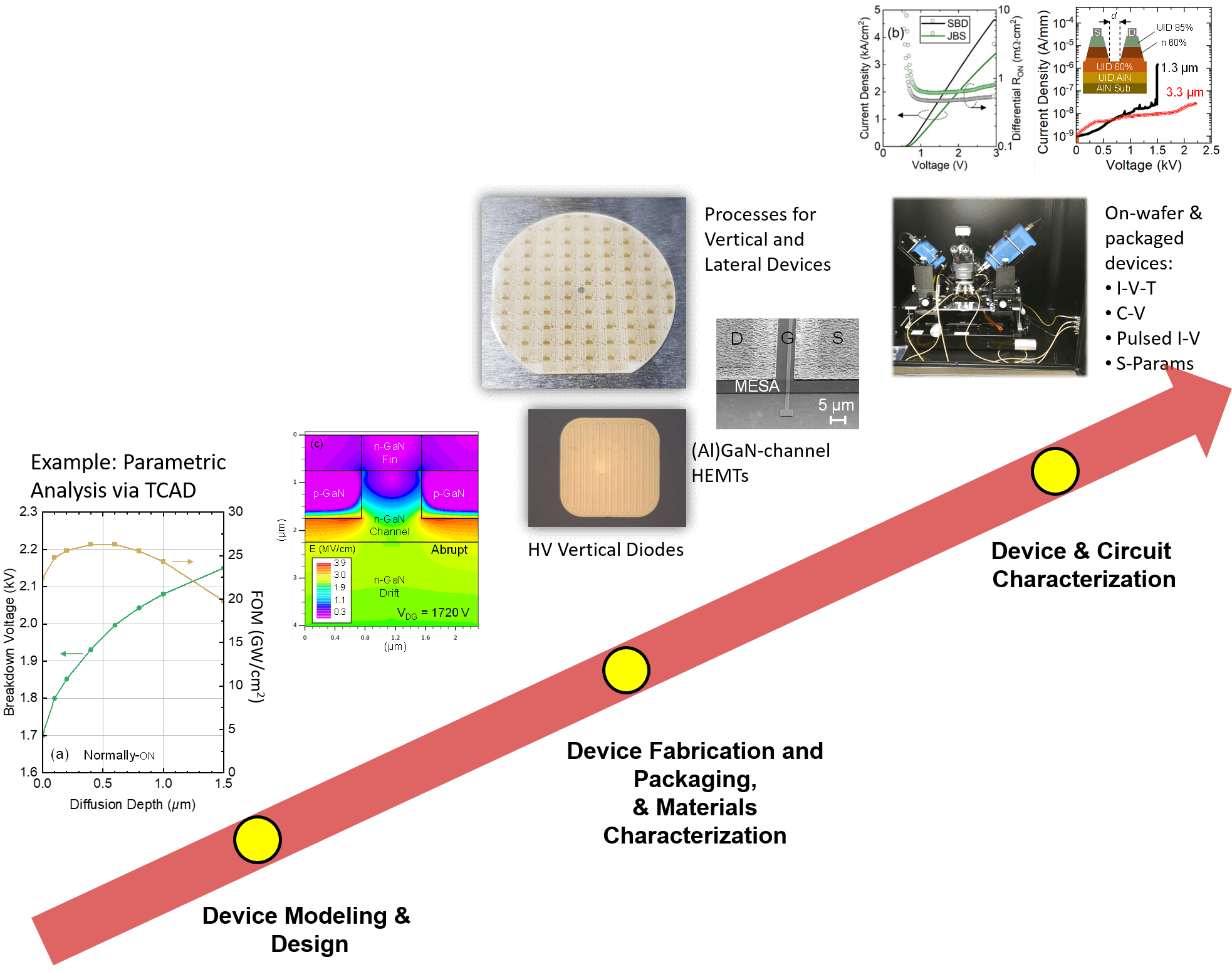
Research on SiC and GaN at CISEDS center will focus on developing new device structures, fabrication techniques, and characterization methods to improve the performance and reliability of these devices. This will include investigating new materials and designs for the SiC and GaN devices, as well as developing new fabrication techniques that can produce high-quality devices with minimal defects. Additionally, the center will also focus on the integration of these devices into systems and applications to demonstrate their potential in real-world scenarios.
In addition, the center will also focus on developing new materials, such as SiC and GaN-based heterostructures, to improve the performance of these devices. Heterostructures can be used to create new device structures that can enhance the performance of SiC and GaN devices by introducing new material properties, such as improved electron mobility, enhanced thermal conductivity, or improved carrier confinement.

Furthermore, the center will also focus on developing new characterization techniques that can be used to understand the properties of SiC and GaN devices. These techniques can be used to measure the electrical and thermal properties of these devices, as well as their mechanical properties, and to understand how these properties change under different operating conditions.
CISEDS’s objective is to mitigate these challenges by developing new device structures, fabrication techniques, and characterization methods to improve the performance and reliability of these devices. Additionally, the center will investigate new materials and designs to optimize the performance of these devices. Finally, the center will also focus on the integration of these devices into systems and applications to demonstrate their potential in real-world scenarios. By addressing these challenges, the CISEDS center aims to accelerate the adoption of Wide Bandgap Semiconductor Devices for Power Conversion and High-Frequency Applications in a wide range of applications.
Overall, the CISEDS center will perform cutting-edge research on SiC and GaN to improve the performance and reliability of these devices and pave the way for their integration into a wide range of power electronic applications.
