Quantum Materials, Heterostructures, and Advanced Characterization Techniques

1. MBE of strongly correlated oxide thin films and heterostructures: Molecular beam epitaxy (MBE) is a powerful technique for growing thin films and heterostructures of strongly correlated oxides. These materials have unique electronic and magnetic properties that are highly desirable for a variety of technological applications. However, growing these materials using MBE can be challenging due to the complex nature of the growth process, and the need for precise control over the growth conditions. The CISEDS center will perform research to mitigate these challenges by developing new growth techniques and strategies to improve the quality and reproducibility of these materials.

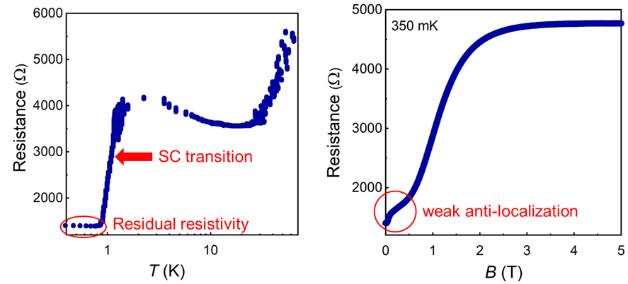
2. Emergent phenomena at the interface of complex oxides: Interfaces between complex oxides can exhibit a wide range of emergent phenomena, such as superconductivity, magnetism, and topological behavior. Understanding these phenomena and how they arise at the interface is a key area of research in the field of condensed matter physics. However, it can be challenging to investigate these phenomena due to the complex nature of the materials and the need for precise control over the interface properties. The CISEDS center will perform research to mitigate these challenges by developing new techniques and strategies to investigate these emergent phenomena.
3. Magneto-electrical effects in thin films and heterostructures: Thin films and heterostructures of magnetic and non-magnetic materials can exhibit a wide range of magneto-electrical effects, such as the spin Hall effect and the anomalous Hall effect. These effects have the potential to be used in a wide range of technological applications, such as spintronics and data storage. However, it can be challenging to investigate these effects due to the complex nature of the materials and the need for precise control over the magnetic and electrical properties. The CISEDS center will perform research to mitigate these challenges by developing new techniques and strategies to investigate these magneto-electrical effects.
4. Advanced gate dielectrics for wide bandgap semiconductors: Wide bandgap semiconductors such as SiC and GaN have the potential to revolutionize electronic devices by offering improved performance and energy efficiency. However, one of the major challenges in developing these devices is the need for high-quality gate dielectrics that can withstand the high-temperature and high-power operation of these semiconductors. The CISEDS center will perform research to mitigate these challenges by developing new gate dielectrics materials and fabrication techniques that are compatible with wide bandgap semiconductors.
The CISEDS center is committed to advancing the state-of-the-art in these areas by investigating new materials, fabrication methods and characterization techniques. In the area of MBE of strongly correlated oxide thin films and heterostructures, the center will focus on developing precise growth techniques and strategies to improve the quality and reproducibility of these materials. This research will help to understand the unique electronic and magnetic properties of strongly correlated oxides and pave the way for their integration into a wide range of technological applications such as spintronics, energy harvesting, and data storage.
In the area of Emergent phenomena at the interface of complex oxides, the center will focus on investigating new techniques and strategies to understand the unique electronic and magnetic properties of these interfaces. This research will help to understand how these properties arise at the interface and pave the way for the integration of these materials into a wide range of technological applications such as high-temperature superconductivity, topological materials, and energy harvesting.
In the area of magneto-electrical effects in thin films and heterostructures, the center will focus on investigating new techniques and strategies to understand the unique electronic and magnetic properties of these materials. This research will help to understand how these properties arise in these materials and pave the way for the integration of these materials into a wide range of technological applications such as spintronics, data storage, and energy harvesting.
In the area of advanced gate dielectrics for wide bandgap semiconductors, the center will focus on developing new gate dielectrics materials and fabrication techniques that are compatible with wide bandgap semiconductors. This research will help to improve the performance and energy efficiency of electronic devices based on wide bandgap semiconductors, such as SiC and GaN. This research will also pave the way for the integration of these materials into a wide range of technological applications such as power electronics and optoelectronics.
Overall, the CISEDS center will perform cutting-edge research in these areas to overcome the challenges and enable the integration of these materials and effects into a wide range of technological applications
