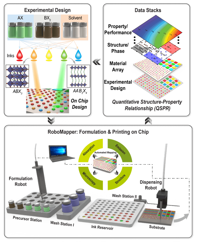
At CISEDS, we are exploring the potential of artificial intelligence (AI) in semiconductor research, opening up new possibilities for the development of new materials and devices. One of the platforms being developed by Dr. Amassian is the RoboMapper and Smart Spin Coater, which utilizes multiple sensors, including optical interferometry, photoluminescence, and computer vision, in combination with AI and decision-making under uncertainty to learn and run multi-objective optimization campaigns. The sensors and AI work together to learn from previous coating runs and autonomously solve coating challenges.
Recently, Dr. Amassian and collaborators were awarded a $7.5M DoD Center for Molecular Doping of Conjugated Polymers, known as the DOPE Center. This funding will enable establishing an entire R&D infrastructure for data-driven research in new materials and devices using the RoboMapper. The team is also building a large database in collaboration with partners to support this work, with a focus on new printed electronics concepts.
We welcome interested members of the IUCRC to visit our Labs to see how sensors and AI work together to learn and solve coating challenges.

Current Printed Electronics R&D mainly relies on manual formulation, printing and evaluation, which can be slow, tedious, repetitive, and incompatible with the digital shift. Additionally, printers and coaters typically operate with only a few discrete materials or formulations at a time, resulting in a bottleneck for new material and device co-design. Automated tools in current R&D often have minimal intelligence, requiring operators to solve problems. The workflow is serial, with excessive operational steps and high costs, time, and environmental footprint for each R&D iteration and prototype.

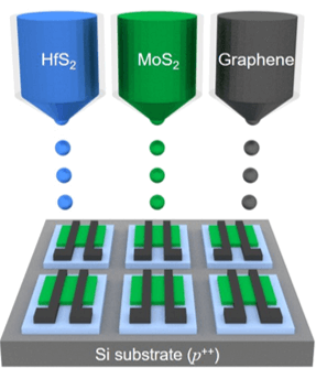
On the other hand, CISEDS Robotic Printed Electronics R&D utilizes automated high-throughput (HT) formulation, printing, and evaluation, which is 10 times faster and fully digitized. It also enables on-the-fly formulation of inks, printing, and coating, including devices, allowing for high-throughput material screening, device prototyping, and co-design. The autonomous and semi-autonomous experimentation with machine learning/AI and inline sensors allows for problem-solving autonomously or with human-in-the-loop. The workflow is parallel, with materials palletization reducing operational steps. The cost, time, and environmental footprint of each R&D iteration and prototype are also reduced by 10-fold, as demonstrated by life cycle assessment (LCA).


