Ultra Wide Bandgap (UWBG) semiconductors are a new class of semiconductor materials that have bandgaps that are significantly wider than those of traditional semiconductors such as silicon and gallium nitride. These materials, such as diamond, AlN, and ZnO, have bandgaps that are several times wider than SiC and GaN, and they have the potential to enable new applications and breakthroughs in power electronics and high-frequency devices.
Research on UWBG semiconductors at CISEDS center will focus on developing new device structures, fabrication techniques, and characterization methods to improve the performance and reliability of these devices. This will include investigating new materials and designs for the UWBG devices, as well as developing new fabrication techniques that can produce high-quality devices with minimal defects. Additionally, the center will also focus on the integration of these devices into systems and applications to demonstrate their potential in real-world scenarios.
In addition, the center will also focus on developing new materials, such as UWBG-based heterostructures, to improve the performance of these devices. Heterostructures can be used to create new device structures that can enhance the performance of UWBG devices by introducing new material properties, such as improved electron mobility, enhanced thermal conductivity, or improved carrier confinement.
Furthermore, the center will also focus on developing new characterization techniques that can be used to understand the properties of UWBG devices. These techniques can be used to measure the electrical and thermal properties of these devices, as well as their mechanical properties, and to understand how these properties change under different operating conditions.

Diamond is also an ultra wide bandgap semiconductor material that has attracted significant attention in recent years due to its exceptional electronic and thermal properties, such as high breakdown voltage, high electron mobility, and high thermal conductivity. These properties make diamond an attractive material for high-power and high-frequency electronic applications, as well as radiation detectors, high-temperature sensors, and high-power electronic devices.
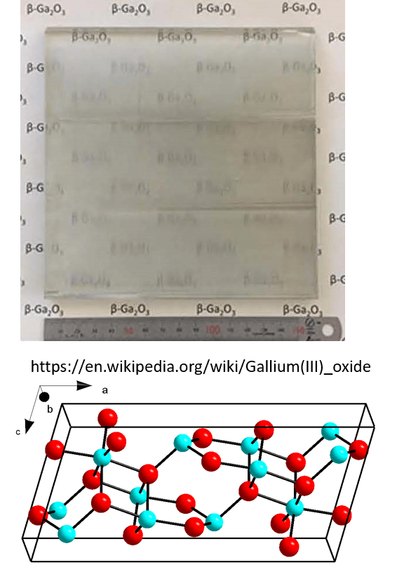
Research on Gallium Oxide and diamond at CISEDS center will focus on developing new device structures, fabrication techniques, and characterization methods to improve the performance and reliability of these devices. This will include investigating new materials and designs for UWBG devices, as well as developing new fabrication techniques that can produce high-quality devices with minimal defects. Additionally, the center will also focus on the integration of these devices into systems and applications to demonstrate their potential in real-world scenarios.
In addition, the center will also focus on developing new materials, such as Gallium Oxide-based heterostructures, to improve the performance of these devices. Heterostructures can be used to create new device structures that can enhance the performance of Gallium Oxide devices by introducing new material properties, such as improved electron mobility, enhanced thermal conductivity, or improved carrier confinement.
Furthermore, the center will also focus on developing new characterization techniques that can be used to understand the properties of diamond and Gallium Oxide devices. These techniques can be used to measure the electrical and thermal properties of these devices, as well as their mechanical properties, and to understand how these properties change under different operating conditions.
Overall, the CISEDS center will perform cutting-edge research on UWBGs to improve the performance and reliability of these devices and pave the way for their integration into a wide range of high-voltage and high-power electronic applications.
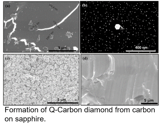
Q-carbon is a novel form of carbon that has been synthesized by scientists at North Carolina State University. It is a highly conductive, durable, and hard material that is created by rapidly heating a carbon-containing material to high temperatures in a controlled environment. Q-carbon has a unique combination of properties, including high electrical conductivity, high mechanical strength, and high chemical stability, which make it a promising material for a wide range of electronic and mechanical applications, such as high-power electronic devices, sensors, and wear-resistant coatings.

Research on Q-carbon at CISEDS center will focus on understanding the fundamental properties of this material, such as its electronic and mechanical properties, and how they can be controlled and optimized. Additionally, the center will also focus on developing new synthesis techniques that can be used to produce high-quality Q-carbon with minimal defects. Furthermore, the center will also focus on developing new characterization techniques that can be used to understand the properties of this material, such as electrical and thermal properties, and how these properties change under different operating conditions.
The center will also focus on the integration of Q-carbon into systems and applications to demonstrate its potential in real-world scenarios, such as high-power electronic devices, sensors, and wear-resistant coatings. This will include the development of new device structures and the characterization of Q-carbon’s performance in these devices, as well as the development of new fabrication techniques that can produce high-quality devices with minimal defects.
