logo
Next-Generation SiC MOSFETs Powering the EV Revolution

Some of the major challenges facing Next-Generation SiC MOSFETs in their efforts to power the electric vehicle revolution include:
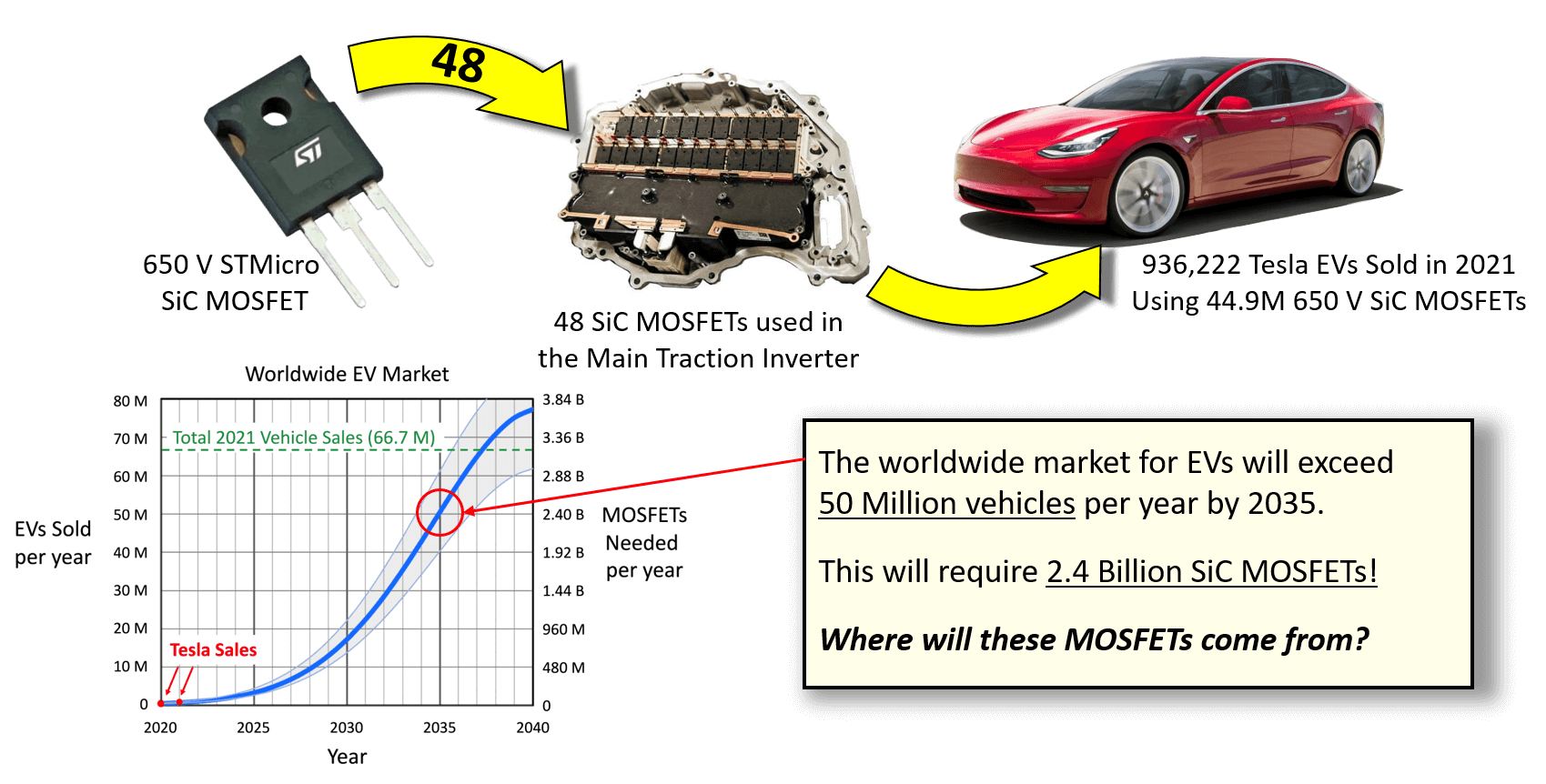
  1. Cost and Scalability: A significant challenge for next-generation SiC MOSFETs is to reduce the cost and increase the scalability of the devices. Research is needed to develop new fabrication techniques and materials that can reduce the cost and increase the scalability of these devices.
  2. Reliability and Durability: Next-generation SiC MOSFETs must be reliable and durable to meet the demanding requirements of electric vehicles. Research is needed to develop new device structures and materials that can withstand the harsh operating conditions of an electric vehicle and maintain their performance over time.
  3. Thermal management: Next-generation SiC MOSFETs achieve high power densities, requiring concentrated heat to be efficiently dissipated to overheating. Research is needed to develop new thermal management techniques to maintain performance.
  4. High-Temperature Operation: Maintaining performance at high temperatures is a significant challenge for next-generation SiC MOSFETs, as they are expected to operate in the high-temperature environment of an electric vehicle. Research is needed to develop new device structures and materials that can withstand high temperatures and maintain performance.
  5. EMI-EMC: SiC MOSFETs are known for their high-frequency switching, which can result in electromagnetic interference. Research is needed to develop new device structures and control strategies that can reduce electromagnetic interference and ensure their compatibility with other electronic systems.
  6. Power losses: The high switching speed of SiC MOSFETs can result in significant switching losses, which can reduce their overall efficiency. Research is needed to develop new device structures and control strategies that can reduce these losses.
  7. High-Voltage Operation: To fully realize the full potential for EV’s to reduce our dependence on fossil fuels, high voltage SiC transistors are required to integrate renewable energy sources such as wind and solar into a modernized electrical grid and to manage grid-scale energy storage. Research is needed to develop new device structures and materials that can withstand high voltage and obtain optimal performance.
Picture3
The CISEDS center has several solutions to the grand challenges facing Next-Generation SiC MOSFETs in their efforts to power the electric vehicle revolution. Some of the solutions include:
Approach 1: MOS interface engineering for increased channel mobility

The first approach for reducing the channel resistance in SiC MOSFETs for EV applications follows a series of steps. The steps include:
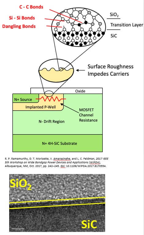
  1. Using oxidation-free gate oxides, such as atomic layer deposition, to reduce the resistance of the channel.
  2. Using low-temperature poly-ox gate oxides that can withstand high temperatures and maintain their performance.
  3. Exploring alternative gate oxide materials that can reduce the resistance of the channel.
  4. Engaging in surface/interface engineering to reduce the resistance of the channel.
  5. Using pre-deposition surface treatment techniques, such as hydrogen etching/termination, silicon-oxynitride termination, etc. to reduce the resistance of the channel.
  6. Using post-deposition annealing to reduce the resistance of the channel.
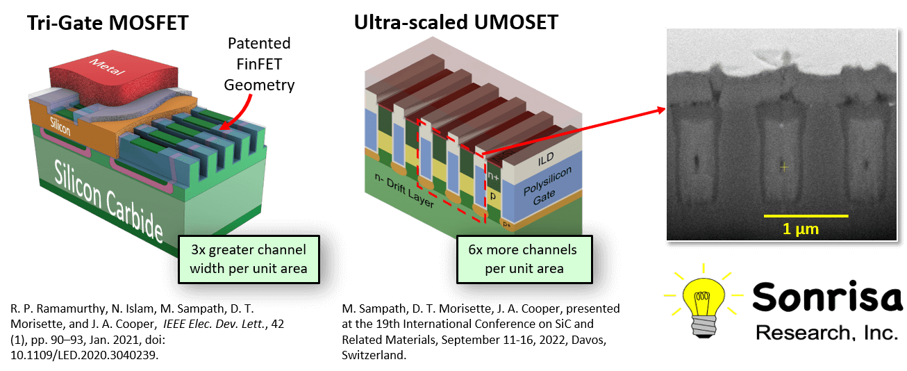
Approach 2: Device engineering for higher channel density
The second approach for reducing the channel resistance in SiC MOSFETs for EV applications is based on Device engineering for higher channel density. This approach involves utilizing techniques to increase the density of the channel in the device, which results in a lower resistance and improved performance.
img
Picture2